
Industry-news
SMD LED APPLICATION NOTES.
STORAGE CONDITIONS
SMD devices are usually moisture/reflow sensitive. Moisture from atmospheric humidity enters permeable packaging materials by diffusion. Assembly processed used to solder SMD packages to PCBs expose the entire
package body to temperature between 160° - 260°. During solder reflow, rapid moisture expansion can result in package cracking, delamination of critical interfaces within the package, or damaged gold wire.
1. Scope: Application notes listed in this document apply to SMD products include the AA, AP, AM, APK, and AT series.
2. Unopened moisture barrier bag (MBB) shall be stored at temperature below 40° with humidity below 90%RH.
3. After the MBB has been opened, the LEDs should be used according to the floor life specified in the table below.
|
LEVEL
|
FLOOR LIFE |
|
|
TIME |
CONDITIONS |
|
|
1 |
Unlimited |
≤ 30°C / 85% RH |
|
2 |
1 year |
≤ 30°C / 60% RH |
|
2a |
4 weeks |
≤ 30°C / 60% RH |
|
3 |
168 hours |
≤ 30°C / 60% RH |
| LEVEL |
FLOOR LIFE |
|
| TIME | CONDITIONS | |
| 4 | 72 hours |
≤ 30°C / 60% RH |
| 5 | 48 hours |
≤ 30°C / 60% RH |
| 5a | 24 hours |
≤ 30°C / 60% RH |
| 6 | Time on Label(TOL) | ≤ 30°C / 60% RH |
4. If the Humidity Indicator Card (HIC)’s 10% mark has changed, or the LEDs have not been used within the floor life specified, they should be baked with the following conditions to reset the floor life:
|
TEMPERATURE |
HUMIDITY |
BAKE TIME |
|
|
When still in carrier tape |
60 ± 3°C |
< 5%RH |
100H |
|
When still in carrier tape |
110°C |
/ |
10H |
5. Do not store LEDs in an environment where high humidity or acidic/basic chemicals are present, as they will
degrade the LED’s metallic surfaces.
6. LED lead frame and soldering pads (cathode and anode) are plated with gold, tin, or other metals. Under long-term exposure to open air, the exposed pins and pads may become oxidized causing poor solderability. Therefore opened but unused parts must be stored in sealed containers. Suggest to store unused parts in the original moisture barrier bag.
7. Moisture control for components already mounted on PCB: If the PCB will not undergo additional reflow soldering or high-temperature processes, then no special treatment is required for the mounted moisture-sensitive SMD components. If the PCB will undergo multiple reflow soldering or other high-temperature processes, including rework, then the SMD component’s cumulative exposure time until the final high-temperature process must be controlled to within the specified time limit.
SOLDERING
1. Do not apply stress to the leads when the component is heated above 85°C, otherwise internal wire bonds may be damaged.
2. SMD products must be mounted according to specified soldering pad patterns. Refer to the product datasheet for details. Solder paste must be evenly applied to each soldering pad to insure proper bonding and positioning of the component.
3. After soldering, allow at least three minutes for the component to cool to room temperature before further operations.
4. The SMD LED Iron Soldering (with 1.5mm Iron tip) condition:
|
SOLDERING IRON |
SOLDERING TEMPERATUR |
MAXIMUM SOLDERING TIME |
|
1.5mm tip size |
<=350°C |
3s |
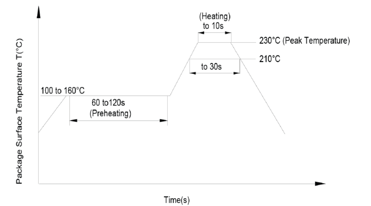
5. Soldering Profile with Pb-Sn Solder
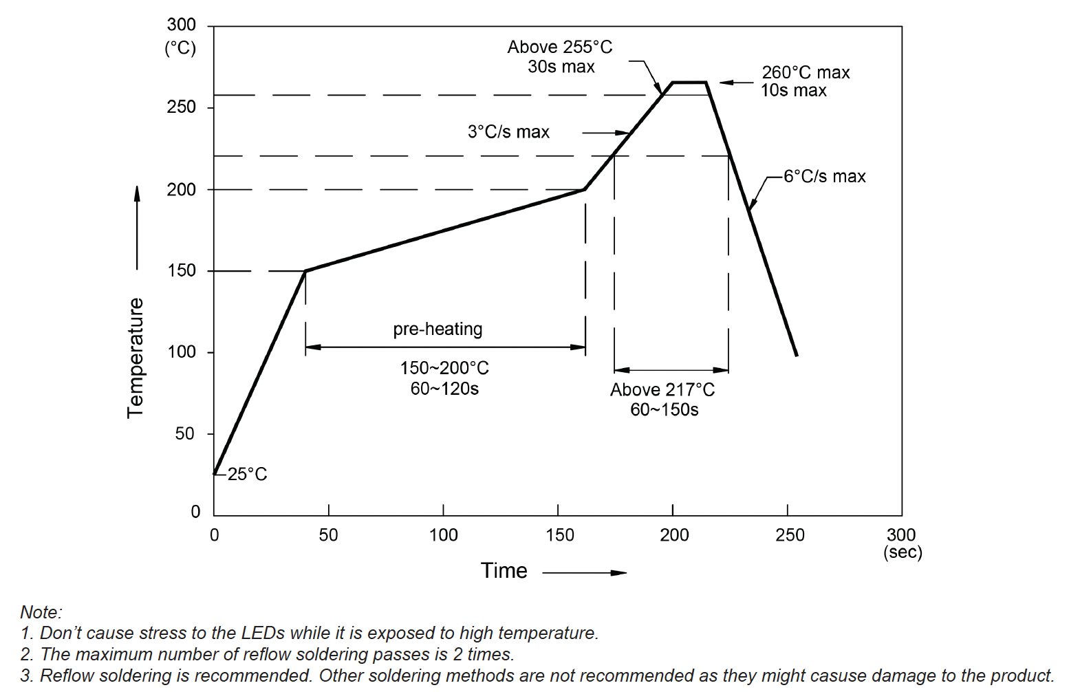
6. Lead-Free Soldering Profile
Note:
1. Don’t cause stress to the LEDs while it is exposed to high temperature.
2. The maximum number of reflow soldering passes is 2 times.
3. Reflow soldering is recommended. Other soldering methods are not recommended as they might cause damage to the product.
7. If component soldering is to be performed more than twice, please consult with ArkTech for suggested conditions.
8. Manual soldering is not recommended unless necessary such as when repair or rework is required.
9. Soldering iron power shall not exceed 30 W. The recommended maximum temperature for lead and unlead soldering is 300°C and 350°C respectively. For blue (typical λd 465 nm), green (typical λd 525 nm), and all white LEDs, the maximum soldering iron temperature is 280°C. Do not place the soldering iron on the component for more than 3 seconds, and the iron should never touch the LED body.
10. For the rework of SMD LED without side surface leads, refer to QFN rework methods. Special atte
ntion should be made for proper thermal isolation of surrounding electronic components.
11. For LEDs with silicone encapsulation such as the AA and AT series, the outer diameter of the pick-up nozzle must be longer than that of the LED’s light emitting area. i. e. A >C, and B shall be shorter than the width of the LED
12. There shall be no gap between the nozzle and the surface of the LED when picking up. It is recommended to use a soft nozzle to avoid damage caused by excessive stress. Slowing down the pick-up process may help if the nozzle is having difficulty picking up the LED.
13. Optimal usage of high-power LED devices requires careful design by the end-user to optimize heat dissipation, such as increasing the size of the metal backing around the soldering pad. Refer to the product datasheet for specific design recommendations regarding heat dissipation.
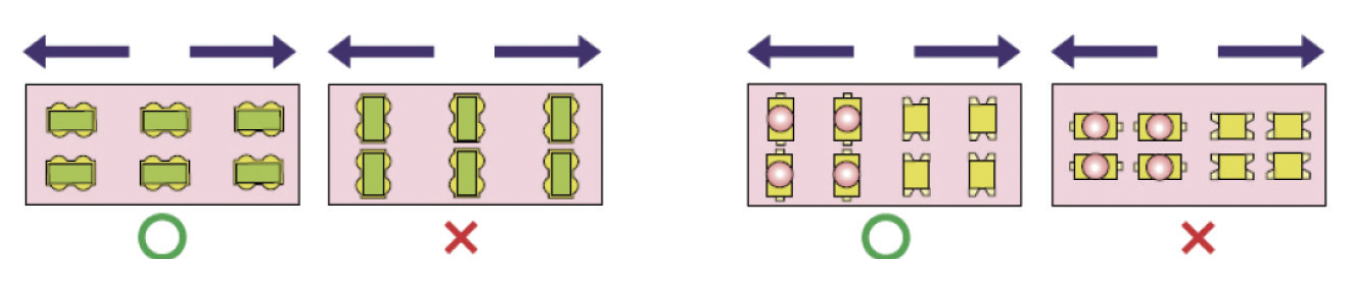
14. During soldering, SMD components should be mounted such that the leads are placed perpendicular to the direction of PCB travel to insure the solder on each lead melts simultaneously during reflow.
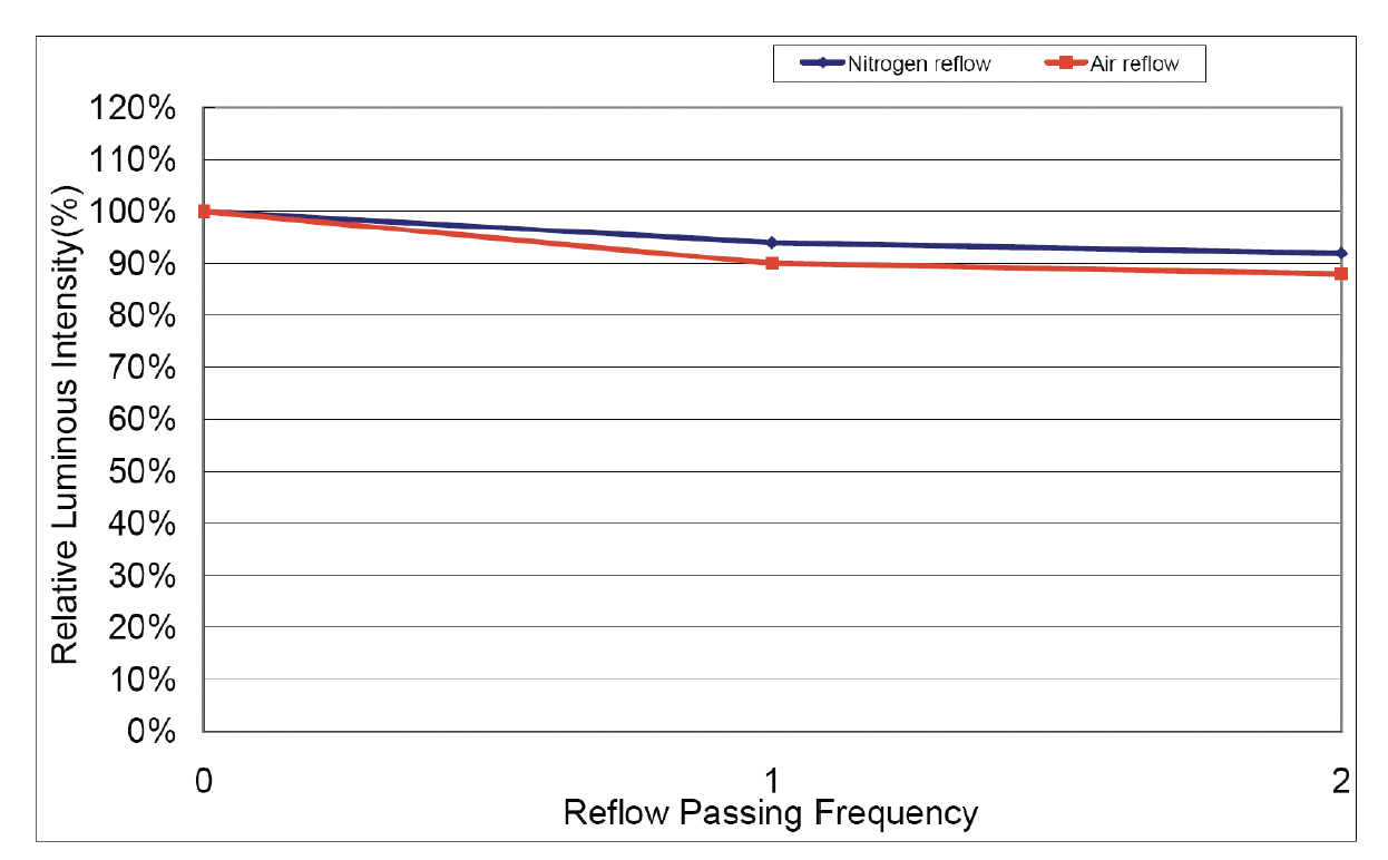
15. Nitrogen reflow soldering is recommended. Air reflow soldering condition can cause optical degradation under the influence of heat and atmosphere. The packaging resin is susceptible to discoloration because of its property change and oxidation under the influence of the heat during the reflow soldering process. Nitrogen reflow can prevent packaging resin discoloration from oxidation and prevent luminous flux decrease. Moreover, nitrogen reflow can prevent solder paste from oxidation, contributing to the improvement of solder wetability. The nitrogen concentration should be increased to approximately 1,000ppm during reflow.
16. Comparison of luminous intensity decrease between air reflow and nitrogen reflow:
17. Notes for PCB singulation after soldering:
a. When separating the soldered PCB into individual assemblies, the board may be subjected to bending tension that could damage the soldered LED components. Please reduce the bending or torsion stress on the board to protect the LED.
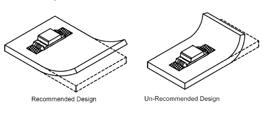
b. The stress on the LED during PCB singulation depends on the position of the LED components on the board. Suggest placing the LEDs at the least stressful areas on the board.
c. Suggest using dedicated jigs to singulate the PCB sheet into individual assemblies. Avoid singulation by hand.
18. For AP series top-firing LEDs, the solder paste should not exceed the thickness of the LED component PCB substrate to prevent excess solder paste from overflowing and seeping under the epoxy lenses, damaging the internal structures during reflow.
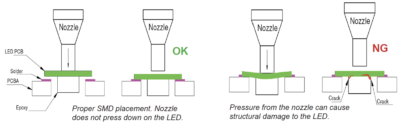
19. When placing reverse-mount LEDs, the nozzle must not place pressure on the part. Refer to the figures below, pressure on the LED will cause the LED to bend and potentially cause delamination or cracking between the component PCB and the epoxy lens. The damaged LED will be more prone to failure after undergoing high-temperature reflow soldering process.
CLEANING
1. Do not use acidic solvents or unknown chemicals to clean the component. Before using any cleaning solvent, check to insure the chemical composition will not corrode or damage epoxy resin, organosilicates, silicone resin, and silver plating, in order to prevent accidental damage or degraded function.
2. Typically we suggest ethanol for cleaning SMD LEDs. Lightly wipe away any surface contaminants and avoid excessive force that might damage the lens surface or internal structures. Allow to dry under room temperature conditions before further usage. Do not soak the SMD LED in ethanol or other solutions.
DESIGN PRECAUTIONS
Products using InGaN / GaN components must incorporate protection circuitry to prevent ESD and voltage spikes from reaching the vulnerable component.
ELECTROSTATIC DISCHARGE PROTECTION
SMD products are electrostatic discharge (ESD) sensitive. Common symptoms observed in an ESD damaged device include unusual forward voltage and reverse current measurements. To prevent devices from being damaged by ESD, please adhere to the advices listed below.
1. Minimize friction between the product and surroundings to avoid static buildup.
2. All manufacturing and testing equipment should be grounded.
3. All personnel in an ESD protected area should wear antistatic garments and wrist straps.
4. Set up ESD protection areas using grounded metal plating for component handling.
5. All workstations that handle IC and ESD-sensitive components must maintain an electrostatic potential of 150V or less.
6. Relative humidity levels maintained between 40% and 60% in production area are recommended to avoid the build-up of static electricity – Ref JEDEC/JESD625-A and JEDEC/J-STD-033.
7. Use anti-static packaging for transport and storage.
8. All anti-static equipment and procedures should be periodically inspected and evaluated for proper functionality.
CIRCUIT DESIGN NOTES
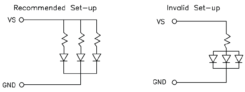
1. Protective current-limiting resistors may be necessary to operate the LEDs within the specified range, otherwise slight voltage shifts will create large current surge and cause burn out failure.
2. LEDs mounted in parallel should each be placed in series with its own current-limiting resistor.
3. The driving circuit should be designed to avoid reverse voltages and transient voltage spikes when the circuit is powered up or shut down.
4. High temperatures can reduce device performance and reliability. Keep LED devices away from heat sources for best performance.
5. It is recommended to operate the LED at the binning current (typ. 20mA) to minimize visible difference in chromaticity and intensity. If the LEDs are to be driven at low current levels (e.g. 2mA), please consult with ArkTech for appropriate design.
6. Excess driving current and/or operating temperature higher than recommended conditions may result in severe light degradation or premature failure.
CATEGORIES
LATEST NEWS
CONTACT US
Name: Ms.Wendy
Mobile:0086-15861679389
Tel:0086-81725657
Whatsapp:0086 17386542651
Email:info@arktechcn.com
Add:8# HengDa CaiFu Center, JinKai Industrial Area, Wuci City, Jiang Su, China