
Industry-news
Application notes for Through Hole LED
Through Hole LED STORAGE CONDITIONS
1. Avoid continued exposure to the condensing moisture environment and keep the product away from rapid transitions in ambient temperature.
2. LEDs should be stored with temperature ≤ 30°C and relative humidity < 60%.
3. Product in the original sealed package is recommended to be assembled within 72 hours of opening. Product in opened package for more than a week should be baked for 30 (+10/-0) hours at 85 ~ 100°C.
4. The LED lead frame surface is plated with silver. When the lead frame is stored under high-humidity environments, or exposed to certain chemical elements or gases, the surface may become discolored. Please maintain the cleanliness of the storage environment.
5. If the storage conditions do not meet specification standards, the component pins may become oxidized requiring re-plating and re-sorting before use. Suggest customers consume LEDs as soon as possible, and avoid long-term storage of large inventories.
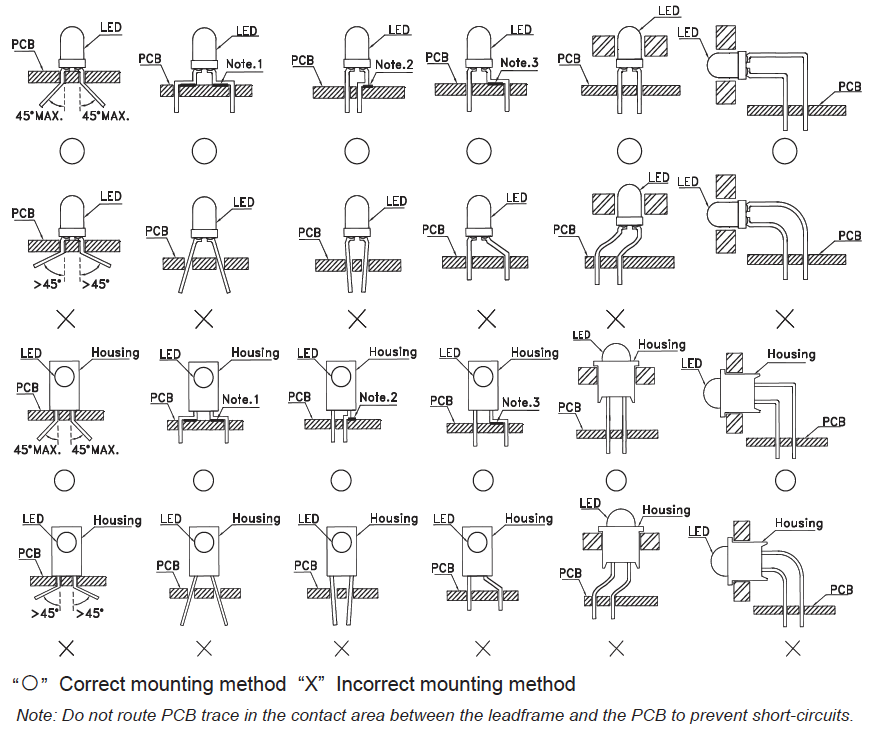
THROUGH HOLE LED MOUNTING METHOD
1. The lead pitch of the LED must match the pitch of the mounting holes on the PCB during component
placement. Lead-forming may be required to insure the lead pitch matches the hole pitch. Refer to the figure below for proper lead forming procedures.
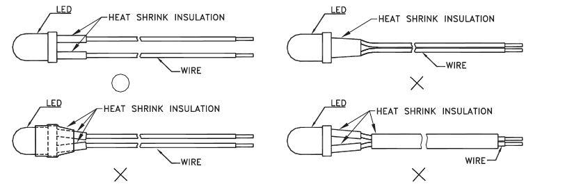
2. When soldering wires to the LED, each wire joint should be separately insulated with heat-shrink tube to prevent short-circuit contact. Do not bundle both wires in one heat shrink tube to avoid pinching the LED
leads. Pinching stress on the LED leads may damage the internal structures and cause failure.
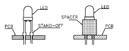
Use stand-offs or spacers to securely position the LED above the PCB.
THROUGH HOLE LED LEAD FORMING PROCEDURES
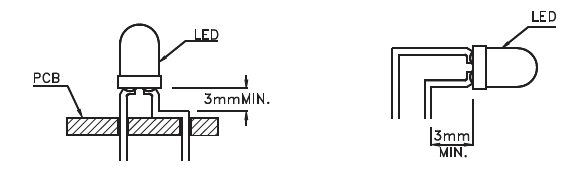
1. Maintain a minimum of 3mm clearance between the base of the LED lens and the first lead bend.
2. Lead forming or bending must be performed before soldering, never during or after Soldering.
3. Do not stress the LED lens during lead-forming in order to prevent fractures in the epoxy lens and damage the internal structures.
4. During lead forming, use tools or jigs to hold the leads securely so that the bending force will not be transmitted to the LED lens and its internal structures. Do not perform lead forming once the component hasbeen mounted onto the PCB. (Fig. 1)
5. Do not bend the leads more than twice. (Fig. 2)
6. After soldering or other high-temperature assembly, allow the LED to cool down to 50°C before applying outside force (Fig. 3). In general, avoid placing excess force on the LED to avoid damage. For any questions, please consult with ArkTech representative for proper handling procedures.
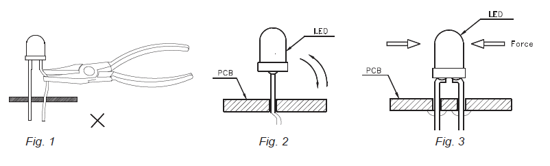
7. When bending the leads, the LED lamp should be secured by the upper part of the lead. Do not grip the epoxy lens during lead-forming bending the lead.
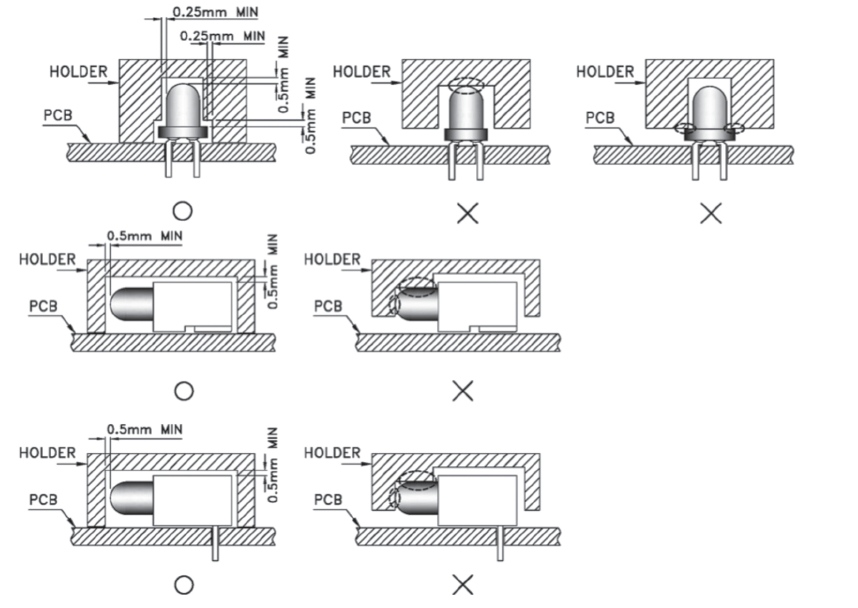
8. During soldering, component covers and holders should leave clearance to avoid placing damaging stress on the LED during soldering.
THROUGH HOLE LED SOLDERING
GENERAL NOTES
1. We recommend manual soldering operations only for repair and rework purposes. The soldering iron should not exceed 30W in power. The maximum soldering temperature is 300°C for Pb-Sn solder and 350°C for lead-free solder for normal lamps and displays. For blue (typical λd 465 nm), green (typical λd 525 nm), and all white LEDs, the maximum soldering iron temperature is 280°C. Do not place the soldering iron on the component for more than 3 seconds.
2. The tip of the soldering iron should never touch the lens epoxy.
3. Do not apply stress to the leads when the component is heated above 85°C, otherwise internal wire bonds may be damaged.
4. After soldering, allow at least three minutes for the component to cool down to room temperature before further operations.
5. Through-hole LEDs are incompatible with reflow soldering.
6. If the LED will undergo multiple soldering passes or face other processes where the part may be subjected to intense heat, please check with ArkTech for compatibility.
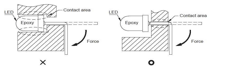
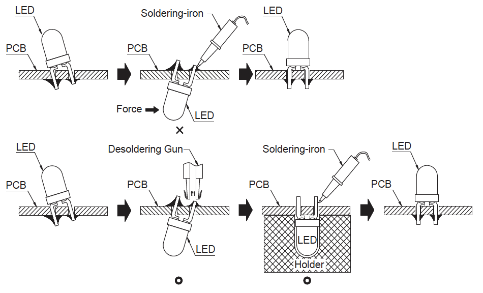
7. In case of misalignment and re-position is required, do not force the LED while applying a soldering iron.
The part should be first de-soldered, and then the LED may be re-soldered with the aid of a holder to place it correctly (as shown below).
RECOMMENDED SOLDERING PROFILE FOR ArkTech THROUGH-HOLE PRODUCTS
1. Iron Soldering (with 1.5mm Iron tip )
|
TEMPERATURE OF SOLDERING IRON |
MAXIMUM SOLDERING TIME |
DISTANCE FROM SOLDER JOINT TO PACKAGE |
|
≤ 350°C |
3S | >2mm |
|
≤ 350°C |
5S | >5mm |
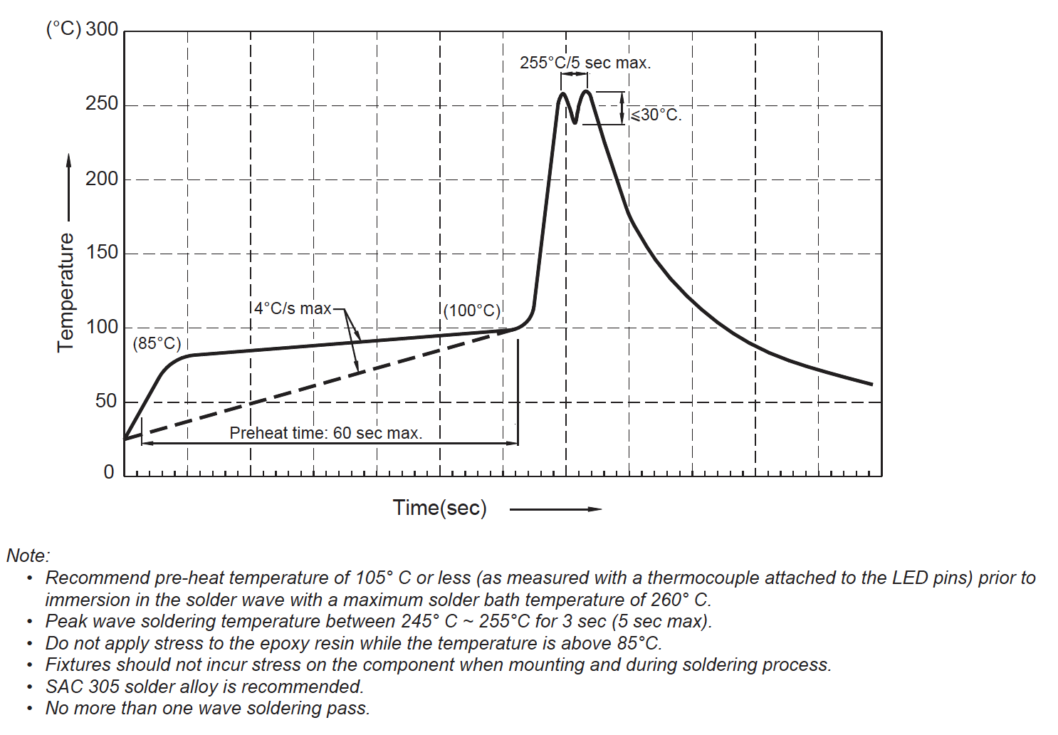
2. Dip Soldering / Wave Soldering
|
TEMPERATURE OF SOLDERING IRON |
MAXIMUM SOLDERING TIME |
DISTANCE FROM SOLDER JOINT TO PACKAGE |
|
≤ 260°C |
3S | >2mm |
|
≤ 260°C |
5S | >5mm |
3. Lead-Free Wave Soldering Profile
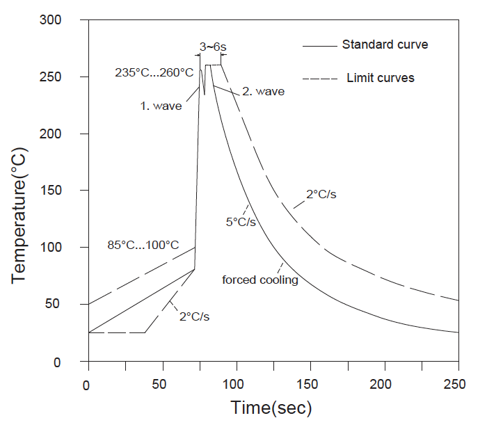
RECOMMENDED REFLOW SOLDERING PROFILES FOR SMD HOUSING LEDS
Lead-Free Reflow Soldering Profile
THROUGH HOLE LED DESIGN PRECAUTIONS
Products using InGaN/GaN components must incorporate protection circuitry to prevent ESD and voltage
spikes from reaching the vulnerable component.
STATIC ELECTRICITY AND VOLTAGE SPIKES IN InGaN / GaN PRODUCTS
InGaN/GaN products are sensitive to electrostatic discharge (ESD) and other transient voltage spikes. ESD and
voltage spikes can affect the component’s reliability, increase reverse current, and decrease forward voltage.
This may result in reduced light intensity or cause component failure.
ArkTech InGaN/GaN products are stored in anti-static packaging for protection during transport and storage.
Please note the anti-static measures below when handling ArkTech InGaN/GaN products.
ESD PROTECTION DURING PRODUCTION
Static discharge can result when static–sensitive products come in contact with the operator or other conductors.
The following procedures may decrease the possibility of ESD damage:
1. Minimize friction between the product and surroundings to avoid static buildup.
2. All manufacturing and testing equipment should be grounded.
3. All personnel in an ESD protected area should wear antistatic garments and wrist straps.
4. Set up ESD protection areas using grounded metal plating for component handling.
5. All workstations that handle IC and ESD-sensitive components must maintain an electrostatic potential of 150V or less.
6. Relative humidity levels maintained between 40% and 60% in production area are recommended to avoid the build-up of static electricity – Ref JEDEC/JESD625-A and JEDEC/J-STD-033.
7. Use anti-static packaging for transport and storage.
8. All anti-static equipment and procedures should be periodically inspected and evaluated for proper functionality.
THROUGH HOLE LED CLEANING
1. Isopropyl alcohol or deionizer water are recommended for cleaning. Do not use acidic solvents or unknown
chemicals, as they might cause corrosion or damage to the component.
2. Lightly wipe away any surface contaminants, and allow the component to dry under room temperature before
further usage. Do not soak the component in solution.
CIRCUIT DESIGN NOTES
1. Protective current-limiting resistors may be necessary to operate the LEDs within the specified range.
2. LEDs mounted in parallel should each be placed in series with its own current-limiting resistor.
3. The driving circuit should be designed to avoid reverse voltages and transient voltage spikes when the circuit is powered up or shut down.
4. The operating current shall not exceed the rated maximum current for the environmental temperature. Please refer to the Current vs. Temperature graph on the datasheet for the current limit at each temperature.
5. Please contact ArkTech representative first if LEDs are to be driven by AC current.DISTANCE FROM SOLDER
JOIN
CATEGORIES
LATEST NEWS
CONTACT US
Name: Ms.Wendy
Mobile:0086-15861679389
Tel:0086-81725657
Whatsapp:0086 17386542651
Email:info@arktechcn.com
Add:8# HengDa CaiFu Center, JinKai Industrial Area, Wuci City, Jiang Su, China